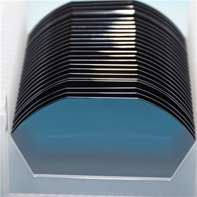
Double Sided Polished Monocrystalline Silicon Wafers
Monocrystalline silicon wafers are usually packaged in air cushion film or foam material to protect their surface finish and integrity.
설명
Description
Monocrystalline silicon wafer has the characteristics of high purity, high crystal quality, low impurity content and good stability. Its surface flatness and photoelectric conversion efficiency are high, which can improve the conversion efficiency of solar cells. In the manufacture of integrated circuits, monocrystalline silicon can improve the performance and reliability of chips.
Specifications:
Monocrystalline silicon wafers are usually specified in terms of diameter and thickness. At present, the diameter of monocrystal silicon sheet can reach more than 300mm, and the thickness can reach tens to hundreds of microns. Different applications require different specifications of monocrystalline silicon wafers.
Specification
| Crystalline structure | Monocrystalline | Notch angle | 90°+5°/-1° |
| Growth Method | Cz | Notch orientation | <100>+-1°or <110>+-1° |
| Dislocation density(oms/cm*3) | Acceptable or None | Rolling | Yes or No |
| Conductance type | P/N | Length(mm) | >=100mm |
| Crystal orientation | 111/100/110 | MOQ(>=200kg) | 380kg/furnace |
| Resistivity(Ω.cm) | 0.001-1000 | Diameter(mm) | Customer standard |
| Dopant | B/P/As/Sb | Oxygen concentration(ppma) | |
| Crystal diameter range(mm) | 100-360 | Carbon concentration(ppma) | |
| Surface metals(oms/cm*2) | <=5E10 | RRG | |
| Notch | SEMI Standard | ORG | |
| Notch depth(mm) | 1.0+0.25/-0.00 | Lifetime(us) |
FAQ
Q: What are your delivery terms?
A: We accept FOB, CIF. CRF EXW according to your request .
Q: What is your normal delivery date?
A: We will deliver the goods with 15 working days after receiving the deposit
인기 탭: double sided polished monocrystalline silicon wafers
문의 보내기
당신은 또한 좋아할지도 모릅니다